An agentic EDA workbench for electronics design.
You describe the board you want, then an agent works through it with you in the browser, from requirements through circuit, schematic and board layout to fab outputs. It stops at each stage for you to sign it off. You can point out problems directly on the schematic or board.
Loom is not publicly available. The repository is private.
Requirements · circuit · schematic · board · design evidence
The Workbench.
SHEET 01 / INTERFACE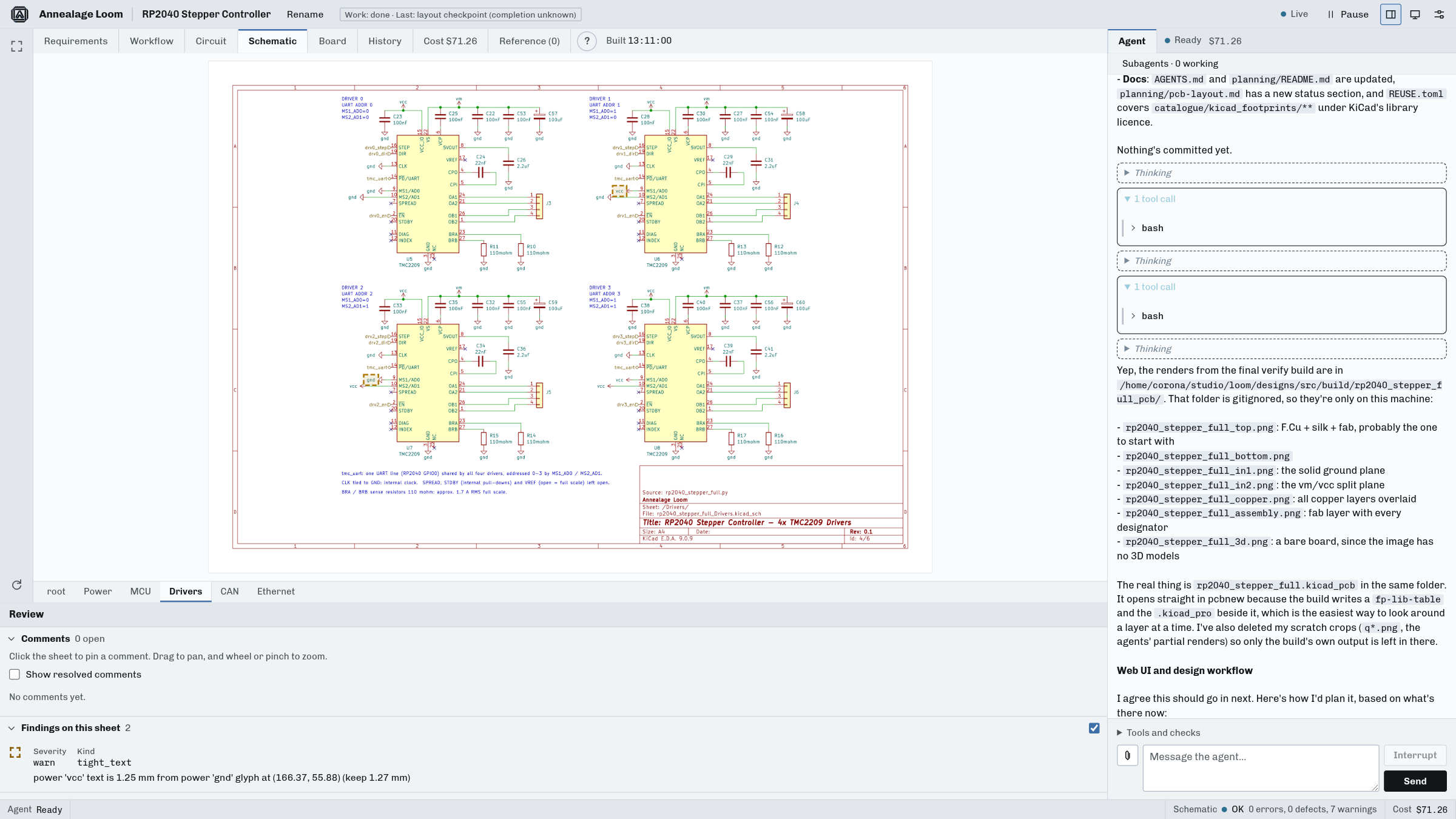
The project page has a tab for each view of the design: Requirements, Workflow, Circuit, Schematic, Board, History, Cost and Reference. A persistent agent pane sits on the right. Review is a button in the title bar, and it shows comments, findings and the build report independently of the chat.
Cost shows agent-reported dollars and tokens by stage and in total. Missing figures remain unknown.
The design moves through eight stages.
SHEET 02 / DESIGN LOOPThe agent stops at each stage for sign-off. Specialist work is limited to a defined scope and checked by a separate reviewer before integration. A checkpoint only records work that's technically complete and matches the current source; unfinished circuit or routing work stays unfinished. Stages close only with current machine evidence and a separate review of the current source.
The Workflow tab shows active work, the last checkpoint, technical completion and optional human acceptance, each separately.
Choose a model at startup in the settings file or on the command line. You can't change it in chat or Settings.
Circuits are checked against their datasheets first.
SHEET 03 / CIRCUIT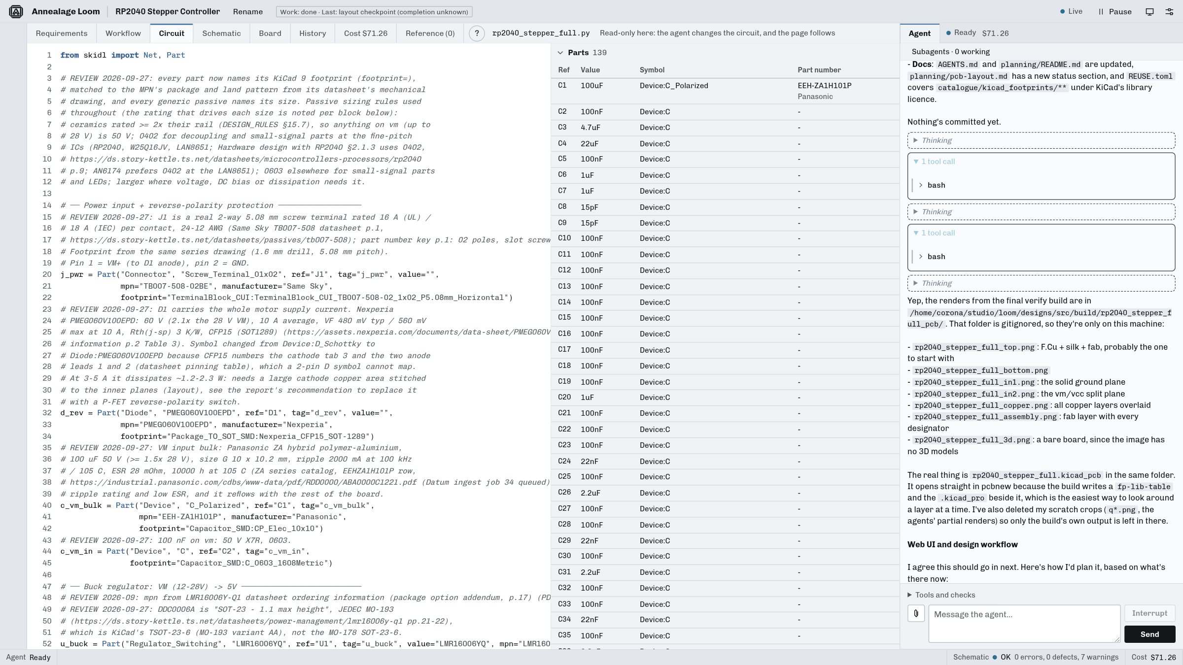
Before anything is drawn, the agent reviews the circuit against each IC's real datasheet: supplies in range, absolute maximums, pin functions, straps and enables tied the way the datasheet asks, the required external parts in place, decoupling at the datasheet's values, the power tree and the value maths. It checks those on the source page, fixes what it can prove is wrong, and writes the evidence into the circuit as a dated REVIEW comment with the datasheet page number.
The datasheet's layout guidance goes in as facts that the board is checked against: a net's current and voltage, a switching regulator's switch node, which nets are analog or fast, and how close a decoupling capacitor has to sit. A hot loop the datasheet warns about becomes a finding on the board.
The circuit is plain SKiDL Python, and every non-generic part carries its manufacturer part number. Datasheets are held in Annealage Datum and looked up by that number. A part that isn't in Datum yet is added through an approval card, which can include a PDF you drop into the chat.
Parts come from KiCad's libraries, or are drawn from the package.
SHEET 04 / SYMBOLS · FOOTPRINTSEvery part needs a symbol and a footprint. The agent searches the stock KiCad 9 libraries first and copies a match into the project, and stock footprints come with their 3D models. When there's no match, it makes the footprint from the dimensions on the datasheet's package drawing. The generator covers chip, dual (SOIC, SSOP, SOJ), quad, PLCC, BGA and through-hole packages, with pads sized by IPC-7351B or as the datasheet draws them, plus an exposed pad with its thermal vias, courtyard, silk and fab layers.
A footprint the agent made is the likeliest place for an error that nobody sees, so the agent doesn't mark its own work. A separate reviewer reads the footprint's source and its rendered preview against the original package drawing, covering pad numbering, positions and sizes, drill shapes, mask and paste, before it goes into the project. Stock footprints get the same independent review. A created footprint gets a plain box for its body in the 3D view, not the manufacturer's model.
The schematic is a sketch file, proved pad for pad.
SHEET 05 / SCHEMATIC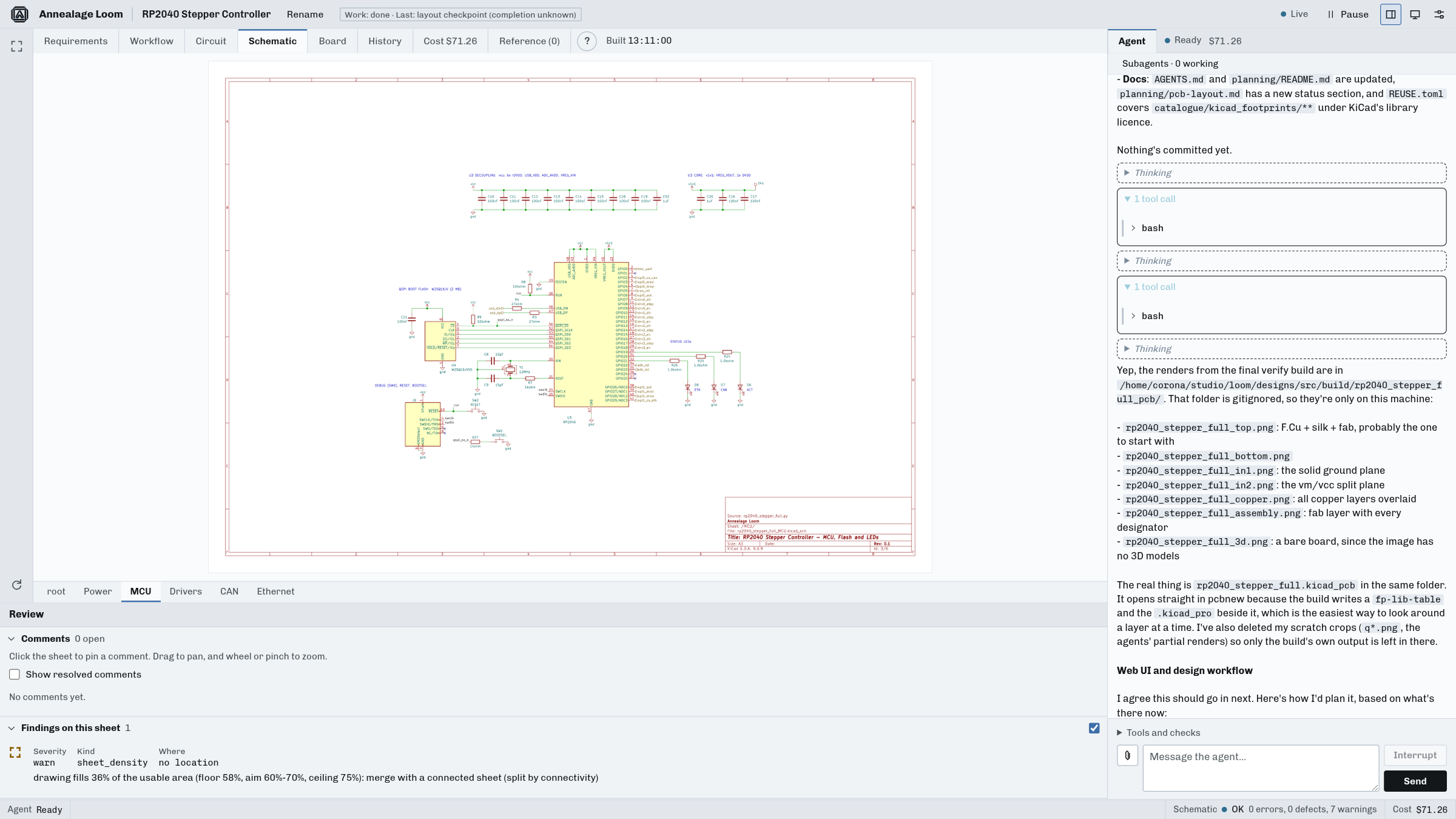
The schematic is a sketch file that records where every part, label and wire goes, one element per line so it diffs well. Every time anything changes, Loom rebuilds the design and proves the drawing against the circuit, pad for pad. A drawing that doesn't match the circuit isn't OK, however nice it looks.
Connectivity is checked pad for pad.
SHEET 06 / DESIGN PROOFThe circuit is the source of truth, and the schematic and board are both drawn from it. The build checks every pad of both against the circuit on every change.
The schematic gets KiCad's electrical rule check on every verified build, along with the drawing lint. The board gets KiCad's design rule check with schematic parity, and it's held to its fab profile. JLCPCB's two-layer and four-layer processes are built in, and a project can add its own.
There is no autorouter and no autoplacer, by design. The agent places every part and draws every wire and track; the tools only measure and check. The engineer signs off the board layout review before routing starts.
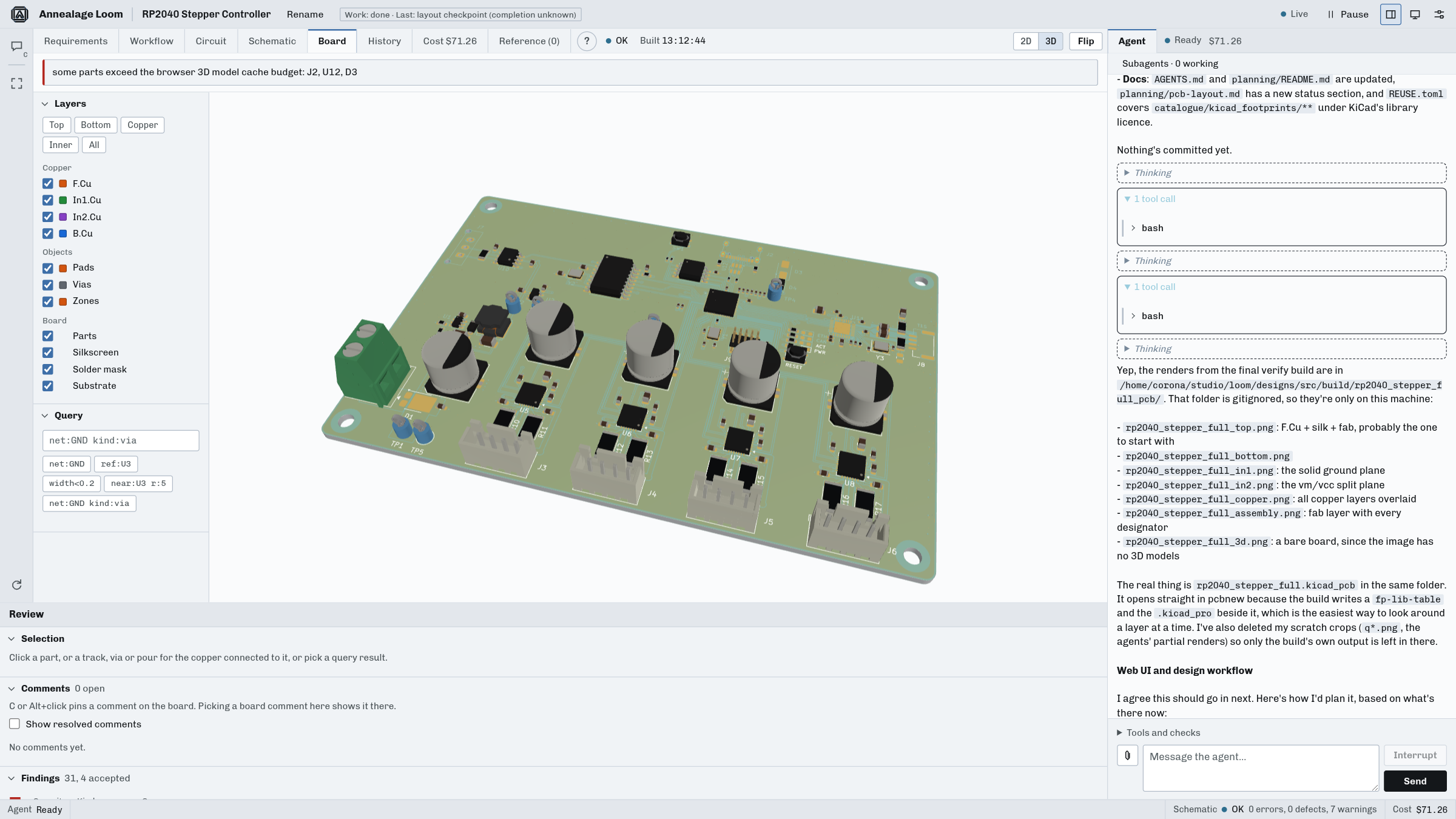
Review the board in 2D or 3D.
SHEET 07 / BOARD REVIEWA board is a layout script beside the circuit. Parts are placed by reference, and every track is drawn from a pad, taking that pad's net. The script can't name a net, so the layout can never add or remove a connection. A track that touches the wrong copper is a short the build reports.
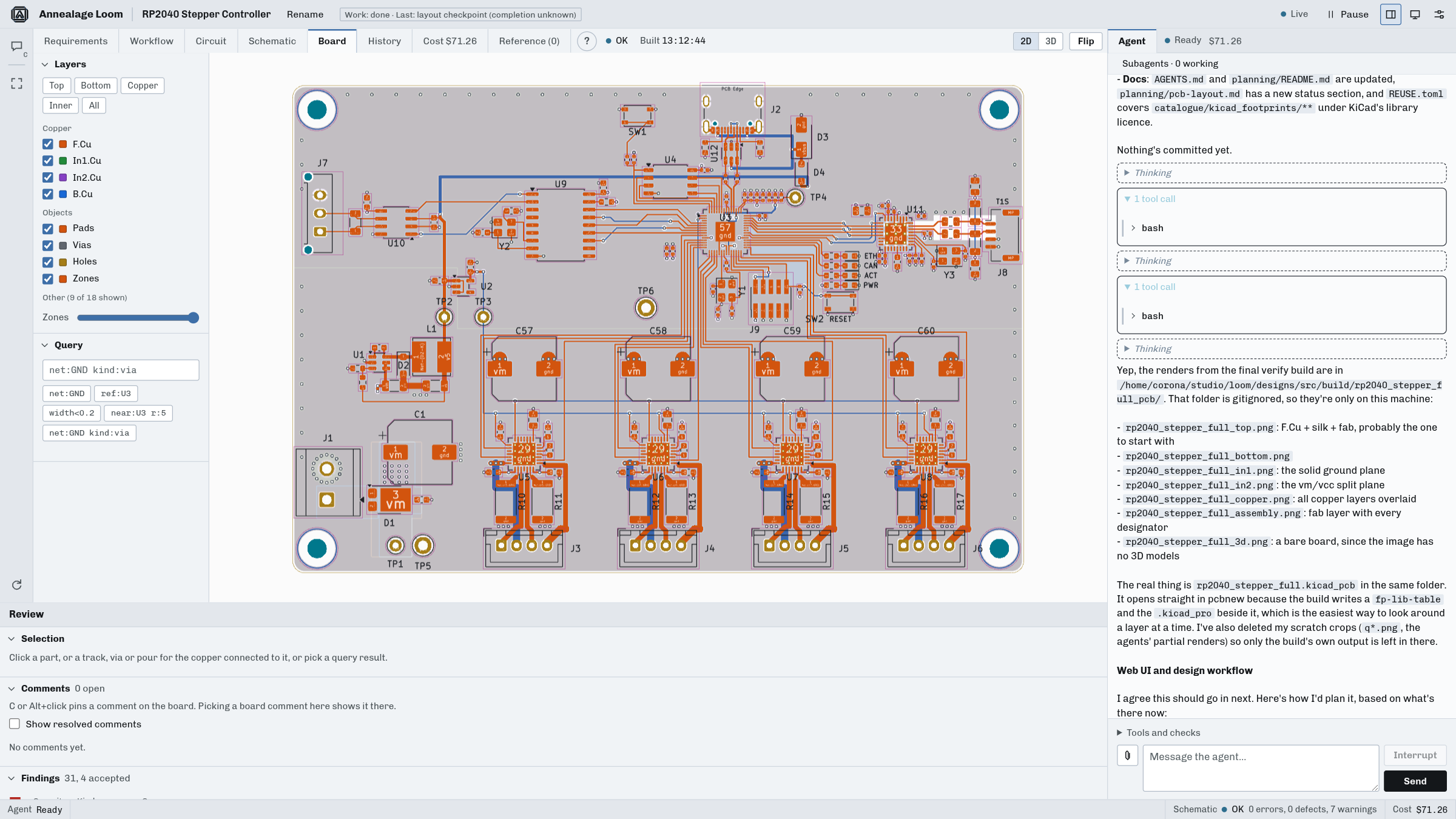
The Board tab has per-layer toggles and click-to-select on parts. Click any track, via or pour to light up all the copper joined to it, in 2D and 3D. This also shows when a net is split.
The query box takes queries such as net:GND kind:via, ref:U3, near:U3 r:5 or conn:U3.12. It uses the same query language the agent uses.
On top of KiCad's checks, the build runs its own layout checks. Track width follows each net's stated current (IPC-2152) and clearance follows its voltage (IPC-2221B). The checks also cover decoupling capacitors at their pins, crystal placement, switching regulator hot loops, return paths under fast signals, test points, connectors on the edge and mounting holes. Buses and differential pairs are checked for skew, spacing, stubs and an unbroken reference plane.
These are layout practice rules for good board design. They are not EMC compliance or a signal-integrity simulation.
When the board is done, the fab export writes Gerbers, drills, a JLCPCB-format BOM and CPL, fab and assembly drawings, an IPC-D-356 netlist and a review packet listing every accepted exception. It is only written after a preflight that rebuilds the nets from the Gerbers and drill files alone and compares them with the circuit.
You steer the design. The agent shows its work.
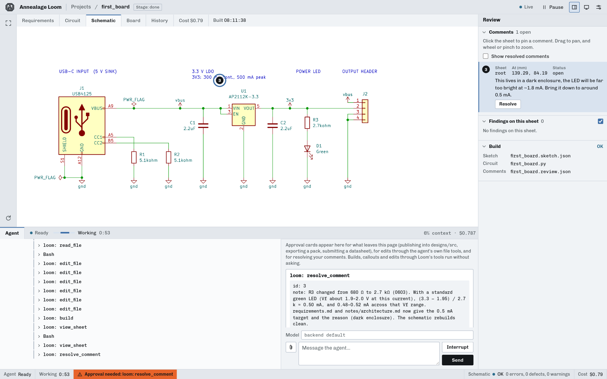
SHEET 08 / REVIEW · APPROVAL · HISTORYClick anywhere on a sheet or the board to pin a comment, type what's wrong and tell the agent. A comment on a part follows the part if a later build moves it. The agent fixes the design, rebuilds, looks at the result, and resolves each comment with a note saying what it did. It pins its own callouts too, when it wants to point at something.
Hit Pause in the title bar and anything that changes the design is refused until you un-pause, so it won't move under you while you're looking. The agent can still read.
Anything that leaves the project asks first, with an approval card that has Allow or Deny. That covers exporting a design pack or fab pack, submitting a datasheet to Datum, and resolving a comment you wrote. A reason on a deny goes back to the agent word for word.
Every design change is a git commit tagged with the turn it came from. History lists each change by turn and author, with its diff, and restores to before any agent turn. Restore is refused while an agent turn runs.